PPT EKT 124 / 3 DIGITAL ELEKTRONIC 1 PowerPoint Presentation, free download ID6216999
A SR latch (R1, R2 = 1 kΩ; R3, R4 = 10 kΩ)In electronics, flip-flops and latches are circuits that have two stable states that can store state information - a bistable multivibrator.The circuit can be made to change state by signals applied to one or more control inputs and will output its state (often along with its logical complement too). It is the basic storage element in sequential logic.
Circuit Designs Of A Sr Latch Along With Its Reversible Truth Table Images
The SR latch truth table and working of the SR latch are given below. Case 1. For the input S=1; R=0, the output of the lower NAND gate is 1. Because from the NAND truth table, even one low input gives you a high output. Thus Q'=1. The input to the upper NAND gate is now 1 NAND 1, which is equal to 0. Q =0.
Basic NAND Gate SR Latch Circuit
Gated D Latch - D latch is similar to SR latch with some modifications made. Here, the inputs are complements of each other. The letter in the D latch stands for "data" as this latch stores single bit temporarily. The design of D latch with Enable signal is given below: The truth table for the D-Latch is shown below:
Logic Diagram And Truth Table Of Sr All Gates My Learning Point / Pls give truth table for
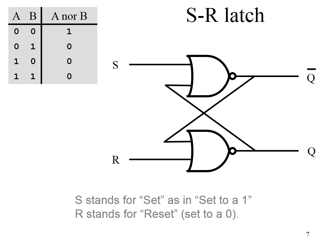
From the above analysis, we obtain the truth table in Figure 4(b) for the NAND implementation of the SR latch. Q is the current state or the current content of the latch and Qnext is the value to be updated in the next state. Figure 4(c) shows the logic symbol for the SR latch. The SR latch can also be implemented using NOR gates as shown in.
Solved SR latch Truth TableSR latch S stands for "Set" as
An active low SR latch (or active low SR Flip Flop) is a type of latch which is SET when S = 0 (LOW). An active low SR latch is typically designed by using NAND gates. The logical circuit for a SR latch is shown below. In the above logic circuit if S = 0 and R = 1, Q becomes 1. Let us explain how. NAND gate always gives output 1 when at least.
Preset and clear operation with SR latch YouTube
SR Latch & Truth table. A Latch is a basic memory element that operates with signal levels (rather than signal transitions) and stores 1 bit of data. Latches are said to be level sensitive devices. Latches are useful for storing information and for the design of asynchronous sequential circuits.

Set Reset Latch Visually Explained With Truth Table and Wave Diagram (Into to Digital Logic Part
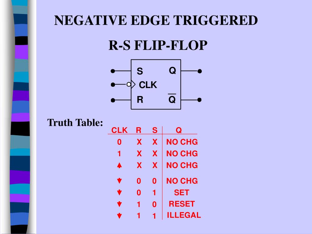
The S-R Latch. A bistable multivibrator has two stable states, as indicated by the prefix bi in its name. Typically, one state is referred to as set and the other as reset. The simplest bistable device, therefore, is known as a set-reset, or S-R, latch. To create an S-R latch, we can wire two NOR gates in such a way that the output of one feeds.

(a) CMIG logical truth table. (b) CMIG logical test results. (c) SR... Download Scientific
sr flip flop:- Latch is basic storage element in which we store 0 or 1. Latch as name suggest it holds 0 or 1. In the circuit "R" stands for reset and "S" stand for set. Q and are the output of the latch. When the circuit will be reset Q value will be equal to 0 and when the circuit will be set the Q value will be equal to 1.

SR Latches, D Latches, and D Flipflops YouTube
Q = 1 and ~Q = 0, just like the truth table. We've acheived the set effect. Proving the other conditions.. Hopefully, by now you have a good grasp on how the SR latch functions as a whole and understand the utility of Verilog when it comes to digital logic design. Here we'll describe the functionality of our SR latch in Verilog, then run.
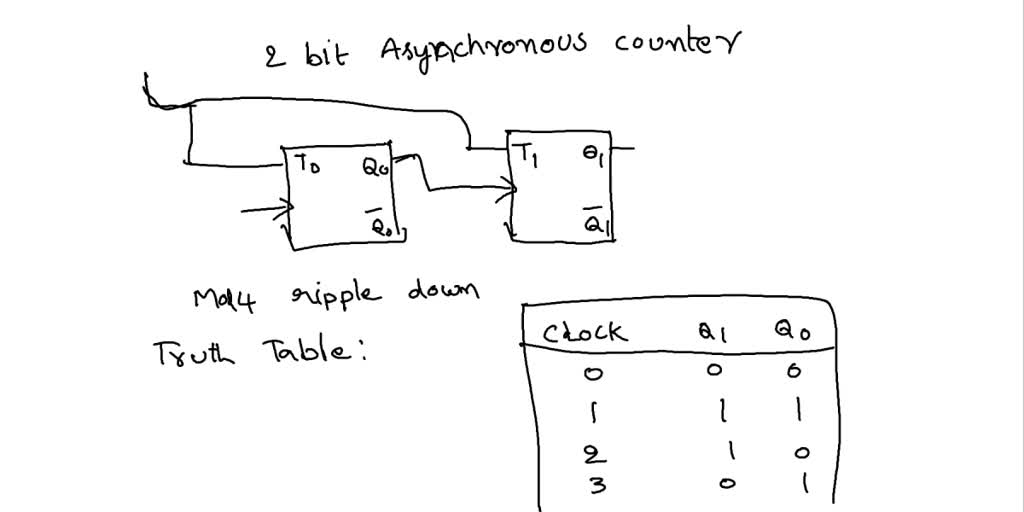
SOLVED '(a) Draw the circuit of 2 bit asynchronous counter with truth table (b) Draw the
S-R Latch truth table. Now, let's analyze how the S-R latch works using its truth table and its circuit with NOR gates. Remember that the NOR gate only gives "1" when both inputs are "0", with any other input combination the output is "0".. As a practical example, you can build an SR latch using the CD4001 chip. Below you can.

SR Latch Behavior and Truth Table Sequential Circuits Explanation — Eightify
Construct a truth table: Create a truth table for the SR latch to illustrate the behavior of the inputs and outputs in different scenarios. 4. Use logic gates to implement the latch: Show students how to use AND, OR, and NOT gates to build the SR latch circuit based on the truth table. 5.

Circuit designs of (a) SR latch along with its reversible truth table... Download Scientific
In this video, the design and working of the SR latch and the Gated SR latch are explained in detail. In the video, the design of the SR Latch using the NOR.

SR Latch NOR and NAND SR Latch YouTube
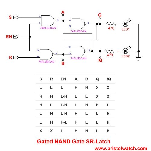
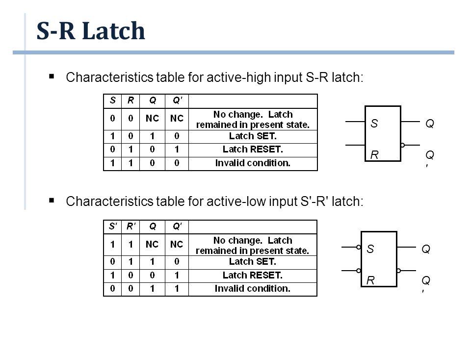
According to the truth table on the right, S and R are active low. When only S is asserted (S is '0'), the output Q is SET to '1'. When only R is asserted (R is '0'), the output Q is RESET to '0'. When neither S and R are asserted, the output holds its previous value. Figure 1. SR-Latch NAND cell. SR-Latch is a kind of bi-stable circuit.
Active high sr latch truth table enjoyfod
The SR Flip-Flop has two inputs( S &R) and two outputs( Q & Q').It is also called a gated or clocked SR latch. It temporarily stores the information of one bit. In digital electronics, a flip-flop (FF) is a 1-bit storage device. It is also known as a bistable multivibrator as it has two stable states, denoted by 0 and 1.

SR LATCH USING NOR GATES TRUTH TABLE EXPLANATION YouTube
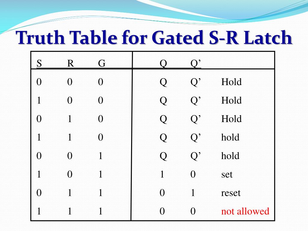
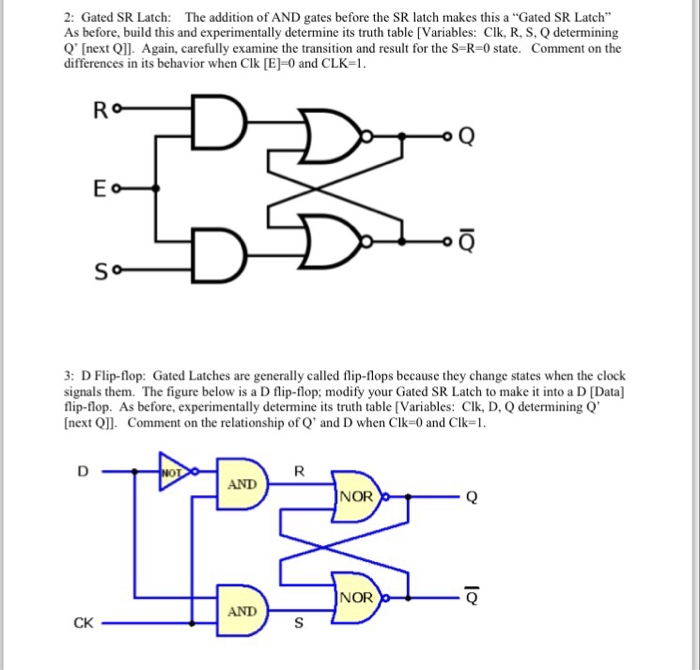
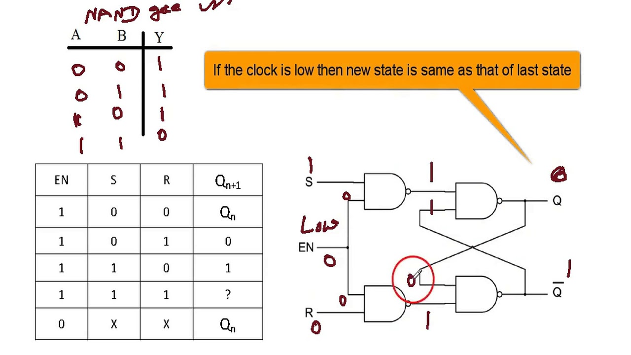
Gated SR- Latch Truth Table . When the E=0, the outputs of the two AND gates are forced to 0, regardless of the states of either S or R. Consequently, the circuit behaves as though S and R were both 0, latching the Q and not-Q outputs in their last states. Only when the enable input is activated (1) will the latch respond to the S and R inputs.
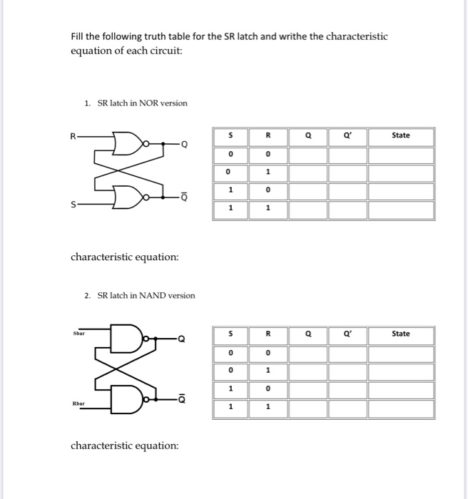
Solved Fill the following truth table for the SR latch and
Learn how SR Latch works with NOR and NAND gates, with clear explanations and diagrams from Neso Academy. Watch the video now.